PCB HDI Technology
In PCB design, the use of HDI technology reduces component packages, routing widths and spacing to create a smaller board size. This, in turn, reduces space occupied by signal paths. It also increases the reliability of your circuits and increases your speed to market. However, achieving the performance benefits of HDI technology comes at a cost. Having tighter requirements in terms of tracing widths, thicknesses and routing locations requires more attention to detail. This can affect the cost of your final product.
Skew in a pcb hdi circuit arises from various sources, including component and interconnect mismatches, signal termination, power rail noise, crosstalk, and other sources. These problems can be mitigated by proper design and manufacturing, but they still exist. Using standard differential or parallel bus delay tuning structures can help compensate for most skew issues and align signals at receiver I/Os.
Other factors can increase the amount of skew in your circuit, including improper component placement and manufacturing defects. This can lead to excessive signal reflections, impedance mismatches and thermal difficulties. Signal skew can be minimized by careful component selection, and by designing your board with a lower layer count to reduce the number of vias required. It is also important to maintain adequate spacing (4 to 8 mil) between traces, and to arrange traces that are susceptible to crosstalk at right angles to each other to reduce coupling. A high copper weight on power and ground planes is also helpful in reducing crosstalk and electromagnetic interference (EMI).
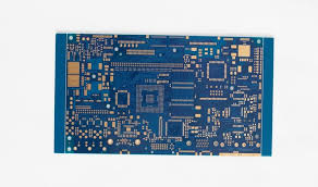
How Does PCB HDI Technology Affect Signal Skew and Jitter?
Jitter occurs when there is a loss of information due to noise and other disturbances. This can result from signal transmission problems or a lack of adequate signal buffering. Jitter can also be caused by the effect of a periodic source, such as switching thresholds and logic thresholds that deviate from their ideal values. It can also be caused by power rail noise or noise induced by the switching of high-speed I/Os.
When properly designed, HDI boards require fewer raw materials owing to their smaller size and low number of layers. This can save on production costs and help to deliver a better performance/value ratio for your end customer. It can also simplify your supply chain and reduce the time to market.
The high-density interconnects on PCB HDI require intricate manufacturing processes to ensure the resulting boards perform properly. These processes involve two key techniques: microvia drilling and sequential lamination. Microvia drilling involves creating small, fine holes to establish connections between different layers on the board. The process uses lasers to achieve a high level of precision. The holes are then filled with plated copper to create a contact surface for component leads. In some cases, the holes can be combined into a via-in-pad design to provide increased contact area and reduce the number of internal layer vias.