Trace Width in Prototype PCB Assembly
A fundamental PCB element, trace width is not only a crucial design factor that impacts signal integrity, but also contributes to the overall functionality and reliability of a circuit board. Narrow traces can overheat and damage both the circuit board and attached components. Wider traces may meet electromigration requirements, but might not allow enough room to route other critical signals. Getting the right trace width is vital for avoiding these types of potential issues, as well as maximizing both current carrying capacity and space utilization.
A number of factors influence trace width, including determining the maximum current that can safely flow through it. In addition, characteristic impedance requirements and routing considerations also factor into the selection of a suitable trace width. Moreover, the size of the copper thickness on a given PCB layer influences a desirable trace width, as do the ratios between dielectric heights and copper thicknesses. Details like pad interfaces, connector densities and pitches also influence the selection of an appropriate trace width, as do matched pair requirements that require smooth neck-downs to control impedance variations.
Other key factors include the type of signal being transmitted, the desired amplitude and frequency, as well as the PCB material and fabrication process constraints. For example, a high-speed signal must be transmitted through multiple layers to reach the destination, while low-power analog and digital signals require careful spacing to prevent coupling noise between fast digital edges and sensitive analog nodes.
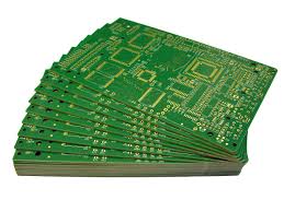
The Importance of Trace Width in Prototype PCB Assembly
Additionally, a PCB’s thermal limitations and component power dissipation also play a role in the choice of a trace width. Excessive heat can cause a variety of problems, from overheating and component damage to instability and reduced lifetime reliability. To help mitigate thermal concerns, designers can employ a variety of techniques, including adding heat sinks and cooling solutions.
In evaluating the above factors, the designer must balance the needs of the circuit board and its manufacturing capabilities against performance objectives. Trace width tradeoffs can be challenging to manage, particularly when it comes to balancing performance objectives across prototype printed circuit board assembly iterations and the production of volume boards.
As such, it’s often best to partner with a PCB layout specialist to ensure that the proper trace widths are selected in line with performance targets throughout the design process. A veteran PCB layout expert can provide professional guidance to help ensure optimal trace width selections aligned with performance objectives across prototyping iterations and volume production. Click here to contact a PCB layout specialist today.
PCB layout software like Altium, OrCAD, and CAM350 make it easy to evaluate and optimize the trace widths of a design before sending it for fabrication. The software’s built-in analysis tools can identify any areas of concern, as well as recommend a solution to avoid these types of issues. In addition, the software can assist with optimizing manufacturing costs by reducing the total amount of copper needed on the board, as well as by identifying traces that are more prone to failure during the etching process.