design considerations are important for an RF PCB
Designing an RF (Radio Frequency) PCB (Printed Circuit Board) involves a unique set of challenges compared to standard PCBs due to the high-frequency signals they must handle. These high-frequency signals, typically operating in the microwave or even millimeter-wave range, require careful attention to detail to ensure signal integrity, minimal interference, and reliable performance. Several key design considerations must be addressed when designing an RF PCB, ranging from material selection to impedance matching, grounding, and minimizing signal reflections. In this article, we will explore the most important design considerations for an RF PCB.
One of the first and most critical design considerations for an rf pcb is the selection of materials. The dielectric properties of the PCB material, such as its dielectric constant (Er), significantly influence the signal propagation speed and impedance characteristics. For high-frequency applications, materials with a stable and low dielectric constant are preferred to reduce signal loss and ensure high-speed signal transmission. Materials like PTFE (polytetrafluoroethylene), Rogers, and other advanced laminates are commonly used in RF PCB design because of their excellent high-frequency performance and low signal attenuation. The choice of material not only impacts signal integrity but also influences the manufacturing cost and complexity of the PCB.
Another essential factor in RF PCB design is ensuring proper impedance matching throughout the circuit. Impedance matching is crucial because an impedance mismatch can lead to signal reflections, which degrade the quality of the signal and reduce the system’s performance. RF transmission lines, such as microstrip or stripline, need to be designed with a consistent characteristic impedance (usually 50 ohms for most applications). To achieve this, designers must carefully select trace widths, the distance between traces, and the thickness of the PCB material. Any variation in these parameters can cause changes in the impedance, leading to reflections and signal loss.
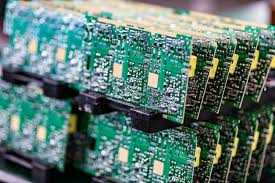
What design considerations are important for an RF PCB?
Grounding is also a critical design consideration for RF PCBs. A poor grounding strategy can introduce noise, signal coupling, and interference, which can significantly degrade the performance of the RF circuit. Effective grounding involves creating a low-inductance ground plane that minimizes the path between ground and the active components, reducing the risk of noise and signal degradation. In many RF PCBs, designers use solid, continuous ground planes that span the entire PCB to provide a stable reference for the signals. Additionally, designers might incorporate via stitching to connect ground planes on different layers of the PCB, further improving grounding performance.
Signal integrity is another significant concern when designing an RF PCB. High-frequency signals are highly susceptible to interference, and ensuring clean, clear transmission is critical. One method of improving signal integrity is to use controlled impedance traces for signal routing. By maintaining a uniform impedance across the entire PCB, designers can reduce signal reflections and loss. Additionally, minimizing trace lengths and avoiding sharp corners in the routing can help reduce the chance of signal degradation. It’s also important to keep traces that carry sensitive signals away from noisy components, such as power lines or high-speed circuits, to prevent interference.
The physical layout of the components is another crucial aspect of RF PCB design. Since RF signals are highly sensitive to their surroundings, careful component placement is necessary to minimize interference and cross-talk between signals. Components such as capacitors, inductors, and resistors must be strategically placed to optimize signal flow and minimize noise. For instance, sensitive components, like low-noise amplifiers, should be placed as close to the input signals as possible to reduce the noise they pick up during signal transmission.
Thermal management also plays a vital role in RF PCB design. High-frequency signals can generate heat, and without proper heat dissipation, the components can overheat, leading to reduced performance or even failure. Designers often use heat sinks, copper pours, or other cooling techniques to ensure that heat is effectively dissipated from power-hungry components. Proper thermal management ensures the longevity and reliability of the PCB.