What is Double-Sided Flex PCB Fabrication?
Double-sided flex PCB fabrication refers to the process of creating flexible printed circuit boards that feature conductive traces on both sides of the flexible substrate. These types of PCBs are ideal for applications that require more complex designs or a higher component density, offering additional flexibility and versatility compared to single-sided flex PCBs. Double-sided flex PCBs are commonly used in industries such as automotive, medical devices, consumer electronics, and wearables. Let’s take a deeper look at the process and benefits of double-sided flex PCB fabrication.
1. Overview of Double-Sided Flex PCBs
In flex pcb fabrication, the term “double-sided” refers to the ability to mount components and route traces on both sides of the flexible substrate. The substrate, typically made of materials like polyimide or polyester, provides the necessary flexibility and durability for the circuit board. In double-sided designs, the traces and components are not only placed on the top side of the board but also on the bottom, allowing for more complex and compact circuit layouts.
This design technique significantly increases the board’s available surface area, making it possible to integrate more components and create more intricate circuits without increasing the size of the board. Double-sided flex PCBs are often used in compact, space-constrained applications where higher functionality is needed.
2. Process of Double-Sided Flex PCB Fabrication
The process of double-sided flex PCB fabrication begins with the preparation of the substrate. The flexible base material is first coated with a thin layer of copper foil, which will be used to form the conductive traces. Then, the design is transferred onto the board using photolithography, a process that involves using light to create a pattern on a photosensitive film.
Once the design is in place, the board undergoes a series of steps, including etching, drilling, and plating, to form the desired copper traces and vias. In double-sided designs, vias (small holes through the board) are used to establish electrical connections between the top and bottom sides of the PCB. These vias are plated to ensure that the circuit is electrically continuous between both sides.
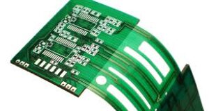
The fabrication process also includes the addition of a coverlay to protect the circuits and ensure the board maintains its flexibility. The coverlay is typically made of polyimide film and is applied over the copper traces, leaving the necessary openings for component mounting and electrical connections.
3. Advantages of Double-Sided Flex PCBs
One of the primary advantages of double-sided flex PCB fabrication is the ability to accommodate more components and create more complex circuits within a smaller footprint. This is particularly useful in applications where space is limited, such as in wearable electronics, smartphones, and compact medical devices.
Another significant advantage is the ability to route electrical traces on both sides of the board, which helps optimize signal flow and minimizes the need for additional layers. This can lead to a more efficient and cost-effective design process, as it reduces the need for multilayer PCBs.
Double-sided flex PCBs also provide greater flexibility and durability. Since the board can bend and flex without compromising its functionality, it is ideal for applications that require dynamic movement or that are subjected to harsh environmental conditions, such as in automotive or aerospace industries.
4. Applications of Double-Sided Flex PCBs
Double-sided flex PCBs are widely used in industries that require compact, high-performance electronics. In the medical field, for instance, these PCBs are used in devices such as hearing aids, insulin pumps, and diagnostic equipment. Their compact design allows for better integration into small medical devices, while their flexibility ensures they can be adapted to fit the contours of the human body.
In consumer electronics, double-sided flex PCBs are used in smartphones, wearables, and other portable devices, where space constraints are a major design consideration. The ability to place traces and components on both sides of the PCB allows manufacturers to create more efficient and functional designs, enhancing the overall performance of these devices.
5. Challenges in Double-Sided Flex PCB Fabrication
While double-sided flex PCB fabrication offers many benefits, it also presents certain challenges. One of the main challenges is ensuring reliable electrical connections between the two sides of the board, especially when dealing with small vias and fine-pitch components. The manufacturing process must be precise to prevent short circuits or weak connections that could lead to failures.
Additionally, the flexibility of the PCB needs to be carefully controlled during fabrication. Over-flexing or uneven bending could cause damage to the traces or components, so careful handling and testing are necessary to ensure that the final product can withstand the required mechanical stresses.
Conclusion
Double-sided flex PCB fabrication offers significant advantages for designing compact, high-density circuits that are both flexible and reliable. By utilizing both sides of the substrate, designers can optimize the available space and create more intricate designs while maintaining the flexibility required for dynamic applications. From wearables to medical devices, double-sided flex PCBs play a crucial role in various industries, enabling the development of innovative, high-performance products. Through careful design and manufacturing, the challenges associated with double-sided flex PCBs can be overcome, making them a valuable solution for today’s advanced electronic devices.